Combinational Logic Circuits using Logic Gates
Combinational circuits are memory less logic gate circuits. It means that output directly depends on the combination of inputs and there is no dependency of outputs in previous input states as in the case of sequential logic circuits. However, these circuits perform a wide variety of electronic operations. This article describes combinational circuits in detail.
Combinational Circuits
Combinational circuits comprise of NAND, NOT and NOR gates connected for producing advanced switching logic circuits. A combinational circuit is one in which several gates have been combined:
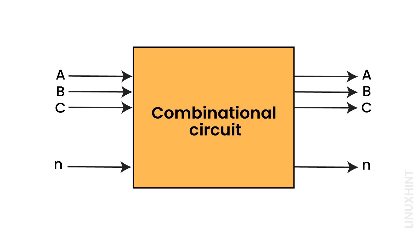
Inputs are represented with A, B, C up to ‘n’ numbers while outputs are represented by A’, B’,C’ up to ‘m’ numbers in the above block diagram.
Common examples of combinational circuits are listed below:
Each of the above combinational circuits are described below.
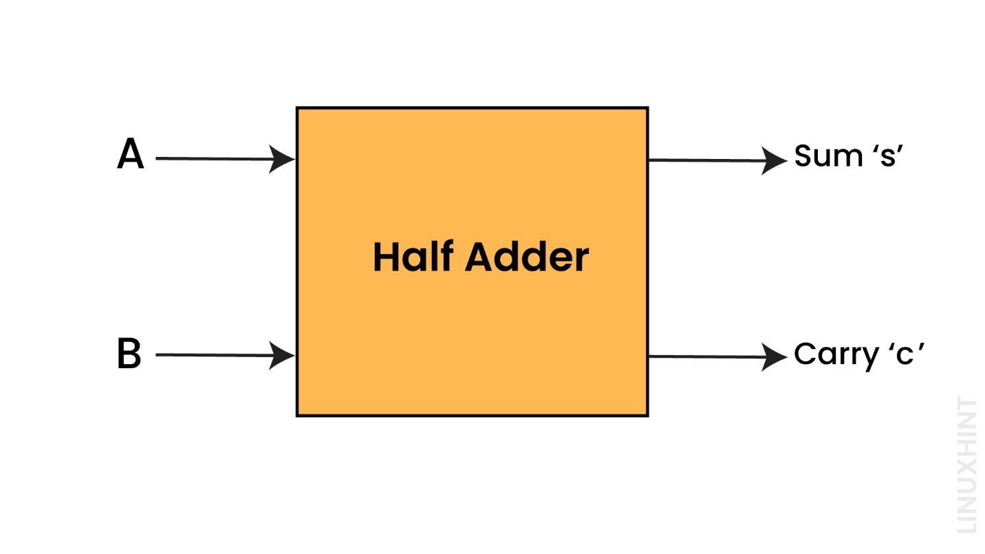
Half Adder
The binary digits A and B, which are both single bits, are supposed to be added by the half adder circuit. It is the fundamental component needed to add two single-bit values. There are two outputs in this circuit: carry and sum.
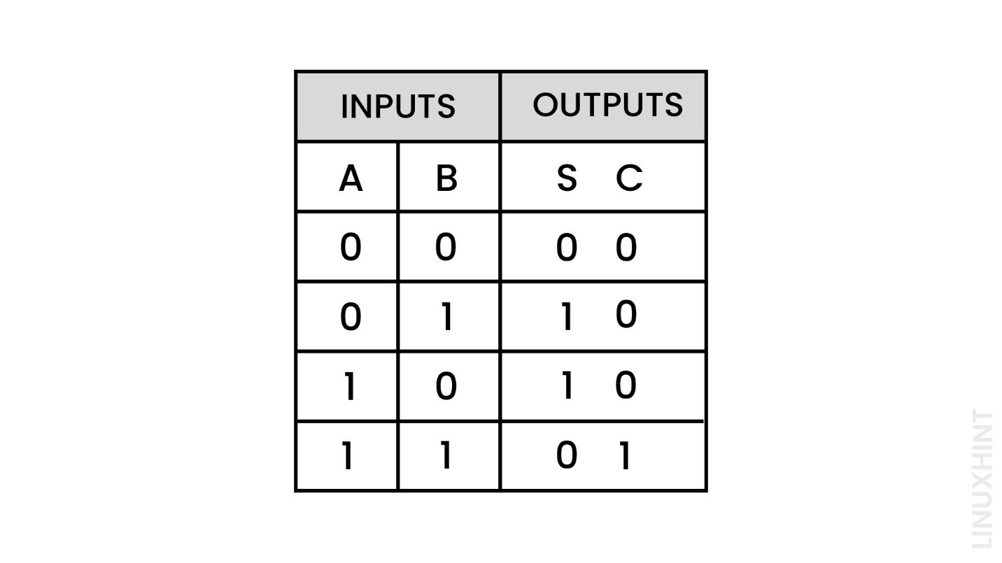
Truth Table
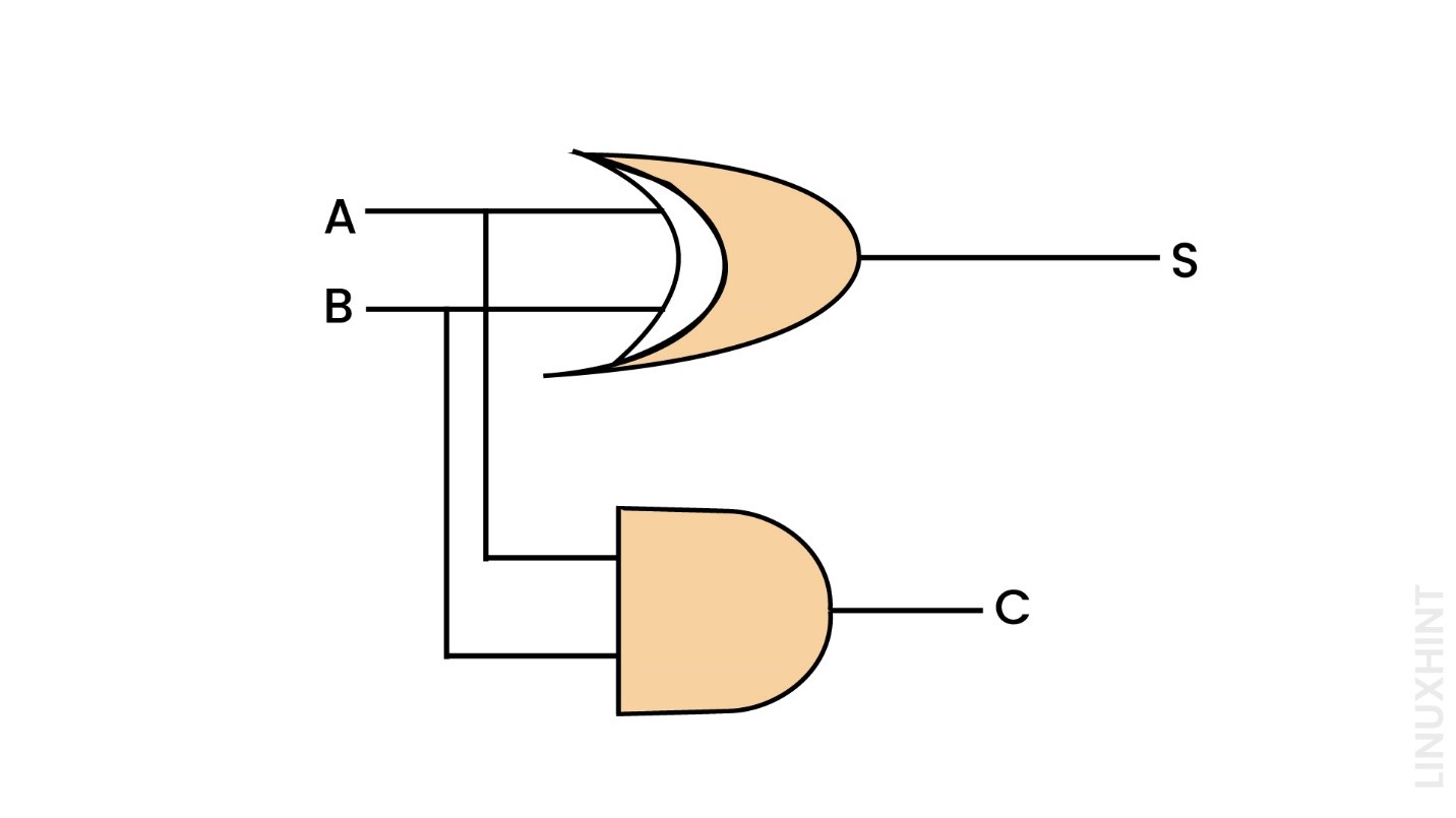
Logical Circuit diagram
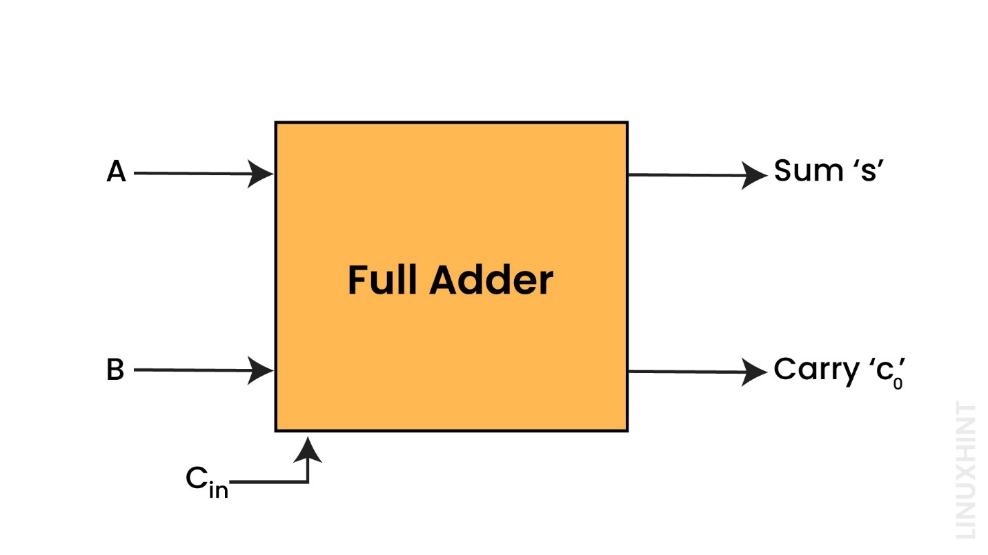
Full Adder
To address the shortcoming of the Half Adder circuit, the Full Adder was designed. It can carry c and add the two one-bit values A and B. The complete adder is a combinational circuit with three inputs and two outputs.
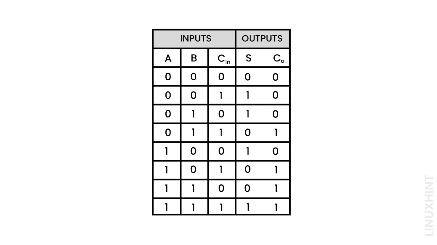
Truth Table
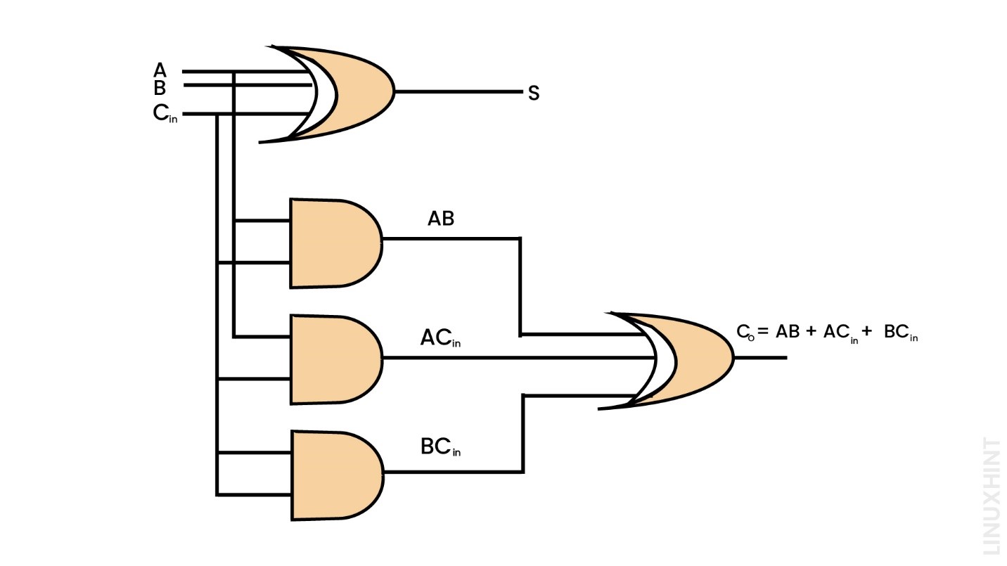
Logical Circuit Diagram
Parallel N-Bit Adder
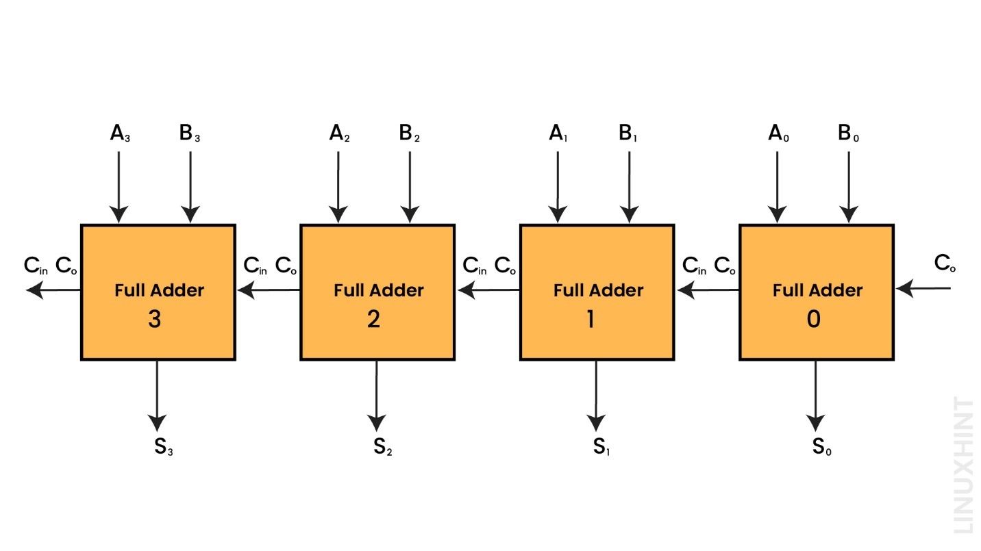
The Full Adder can only add two binary numbers with one digit each and a carry input. However, adding binary integers that are considerably longer than simply one bit is necessary in practice. We need to utilize the n-bit parallel adder to combine two n-bit binary values. It employs a series of cascading full adders. The next full adder’s carry input is linked to the preceding full adder’s carry output.
Parallel 4 Bits Adder
The LSB of the four-bit words A and B are shown in the block diagram as A0 and B0 hence, Stage 0 of Full Adder is the lowest. As a result, its Cin has always been set to 0. The remaining connections are identical to those of the n-bit parallel adder in figure. Among logic circuits, the four-bit parallel adder is highly popular.
N-Bit Parallel Subtractors
By taking the complement (1’s or 2’s) of the integer to be subtracted, the subtraction may be done. As an example, we may subtract (A-B) by adding B’s 1st or 2nd complement to A. That implies that we can execute the binary subtraction using a binary adder.
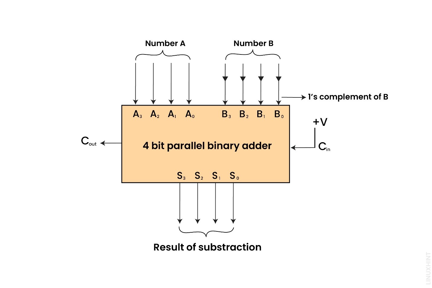
Parallel 4 Bits Subtractor
The number (B) that has to be subtracted is first run through inverters to get its complement, which is 1. A and B’s complement is then added by the 4-bit adder to create the subtraction. The output of binary subtraction (A-B) and carry is represented by the symbols S3 S2 S1 S0. Cout symbolizes the outcome’s polarity. If A > B, then Cout = 0 and the binary form of the result (A-B) is in the form of the 2’s complement. Otherwise, Cout = 1.
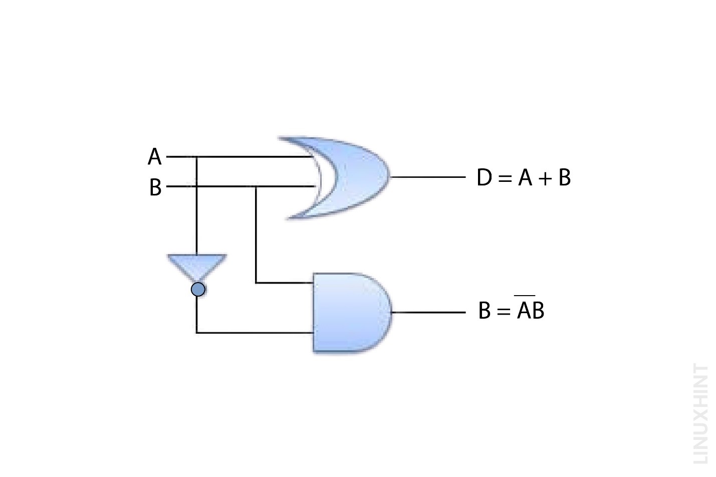
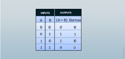
Half Subtractors
Half subtractor has two numbers of inputs and two numbers of outputs and the output (Borrow) shows if a 1 has been borrowed and whether the difference of two binary bits have been supplied. A is referred to as the bit being subtracted in the subtraction (A-B), while B is referred to as the bit that is to be subtracted.
Truth Table
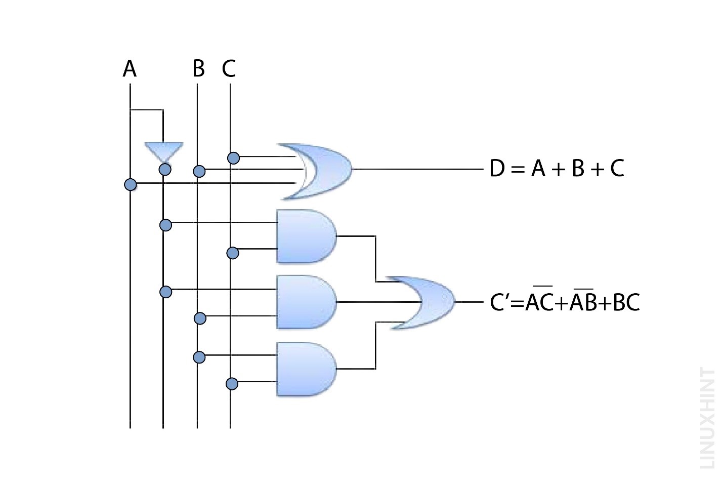
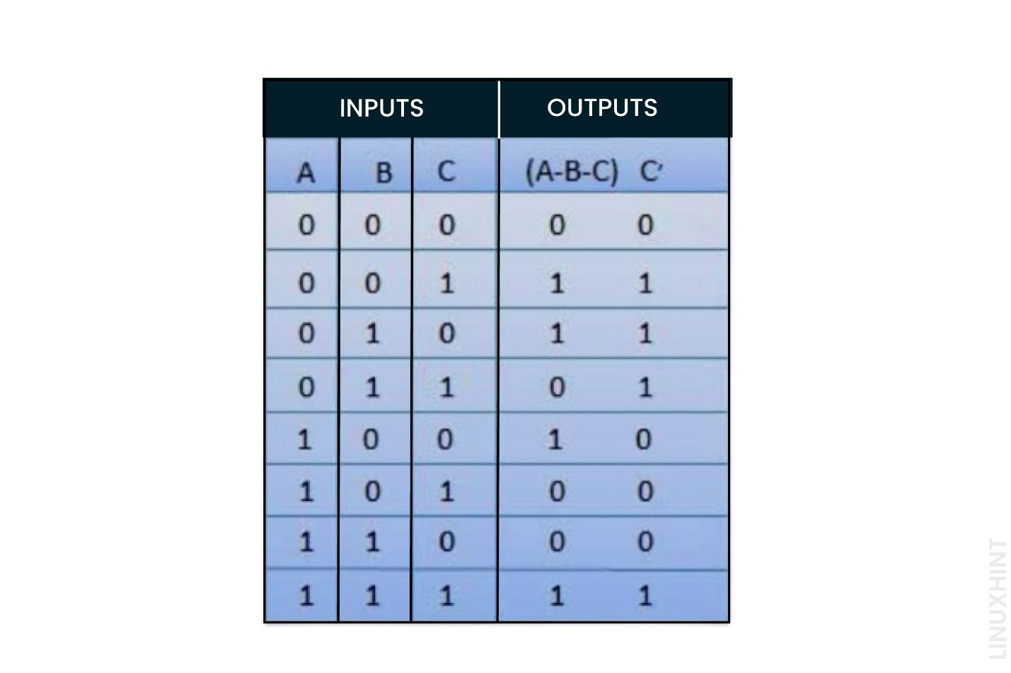
Full Subtractors
A complete subtractor overcomes the drawback of a half subtractor. Three inputs (A,B,C), two outputs (D,C’), and a combinational circuit make up the complete subtractor. A is the one which is being subtracted, B is the number to be subtracted’, C is the ‘borrow’ created by the prior stage, D stands for difference output, and C’ stands for borrow output.
Truth Table
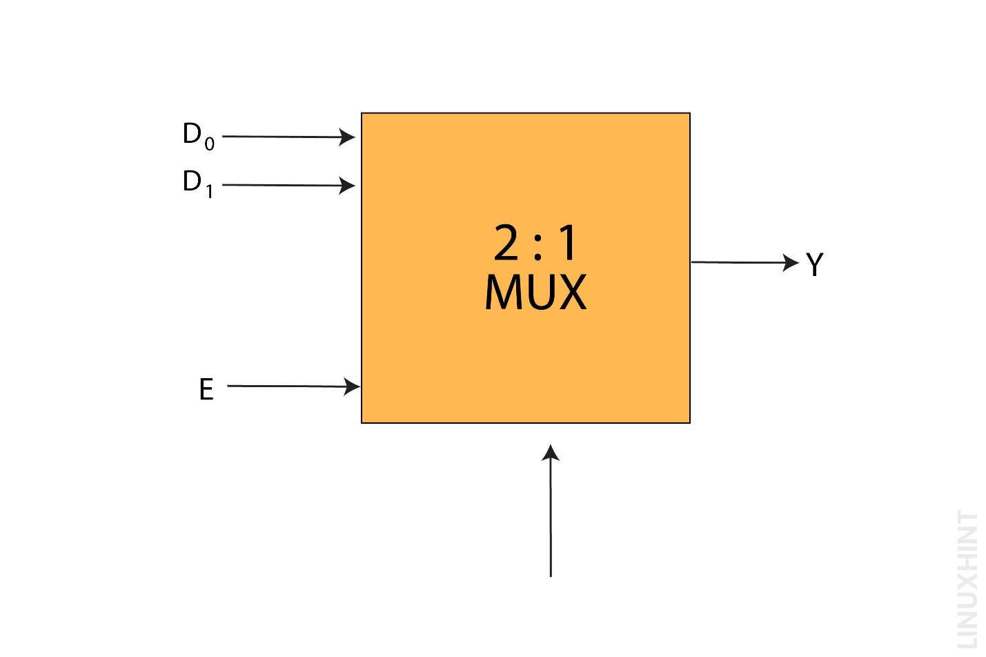
Multiplexers
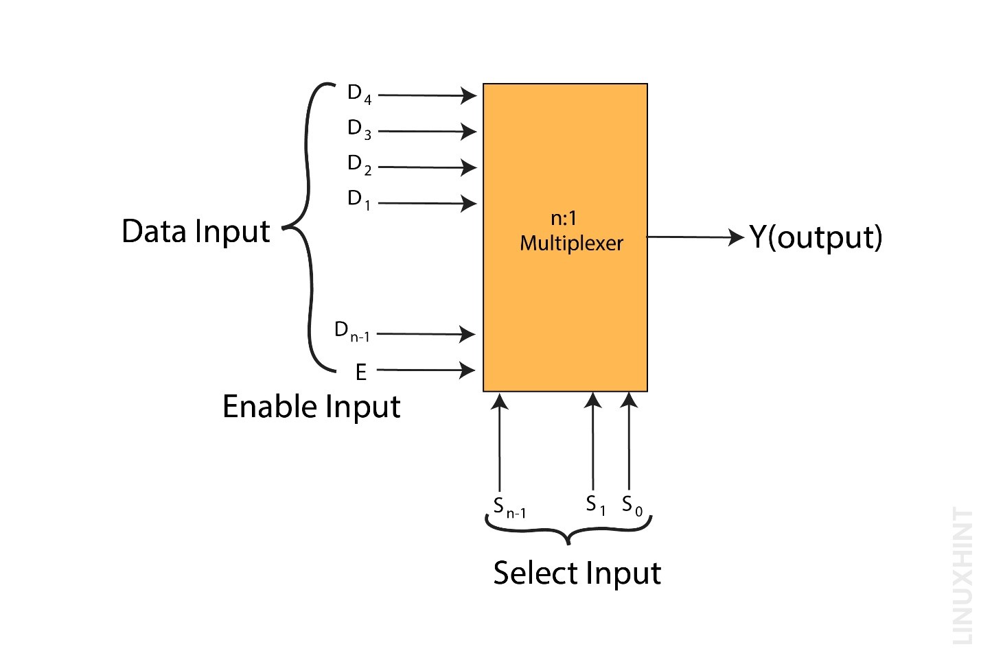
A particular kind of combinational circuit is called a multiplexer. One output, m selects inputs, and n data inputs are present. 2m = n. One of the n data inputs is chosen by the digital circuit, which then sends that data to the output. The chosen inputs decide which one of the n inputs to choose. One out of n data sources is chosen and sent to the single output, depending on the digital coding used at the chosen inputs. Typically, it is an active low terminal, which means that when it is low, it will carry out the necessary action. There are several types of multiplexers configurations: Multiplexer 2:1, Multiplexer 4:1, Multiplexer 16:1 and Multiplexer 32:1.
Block Diagram of a 2:1 Multiplexer
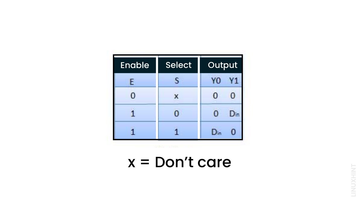
Truth Table of 2:1 Multiplexer
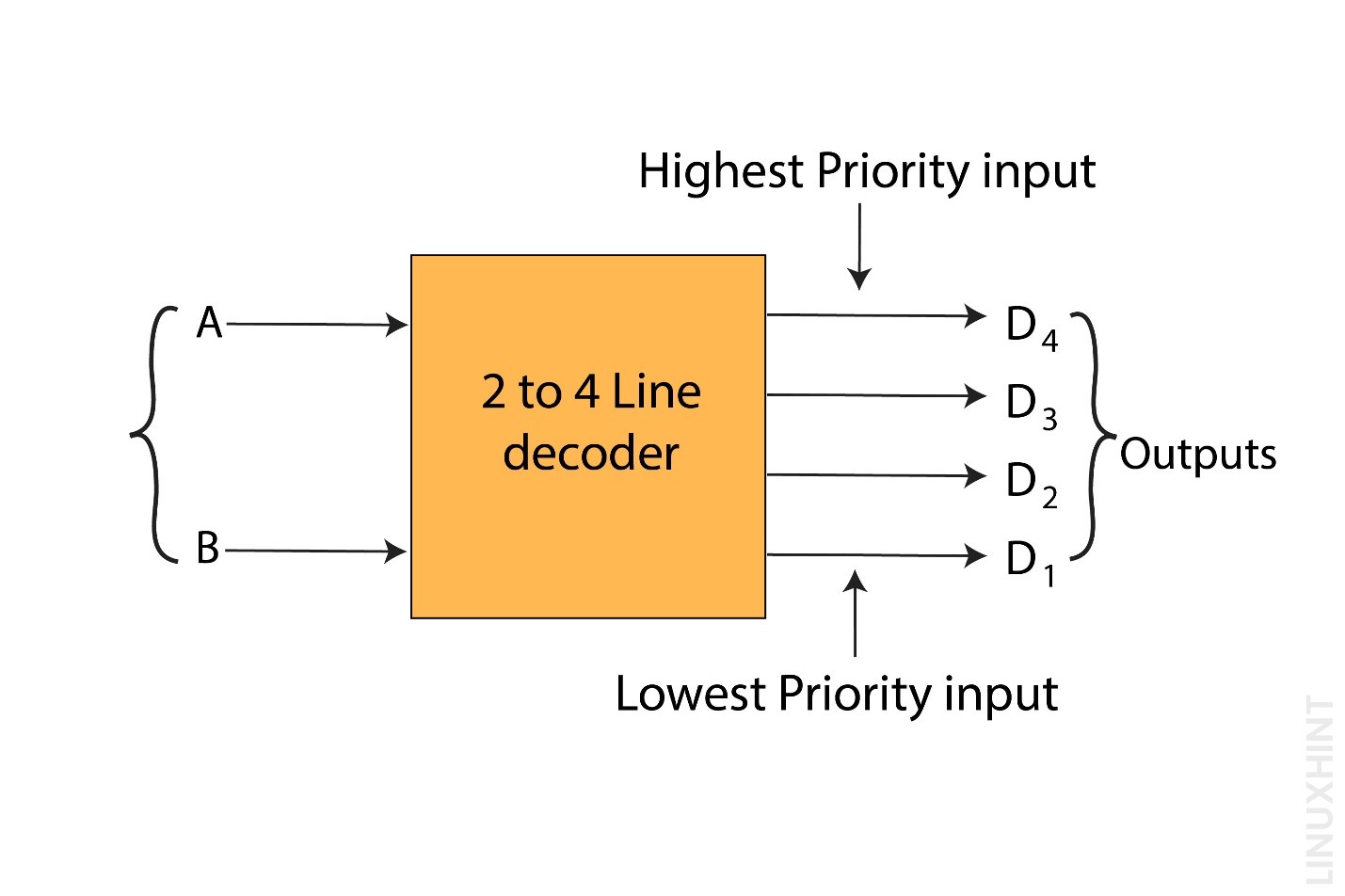
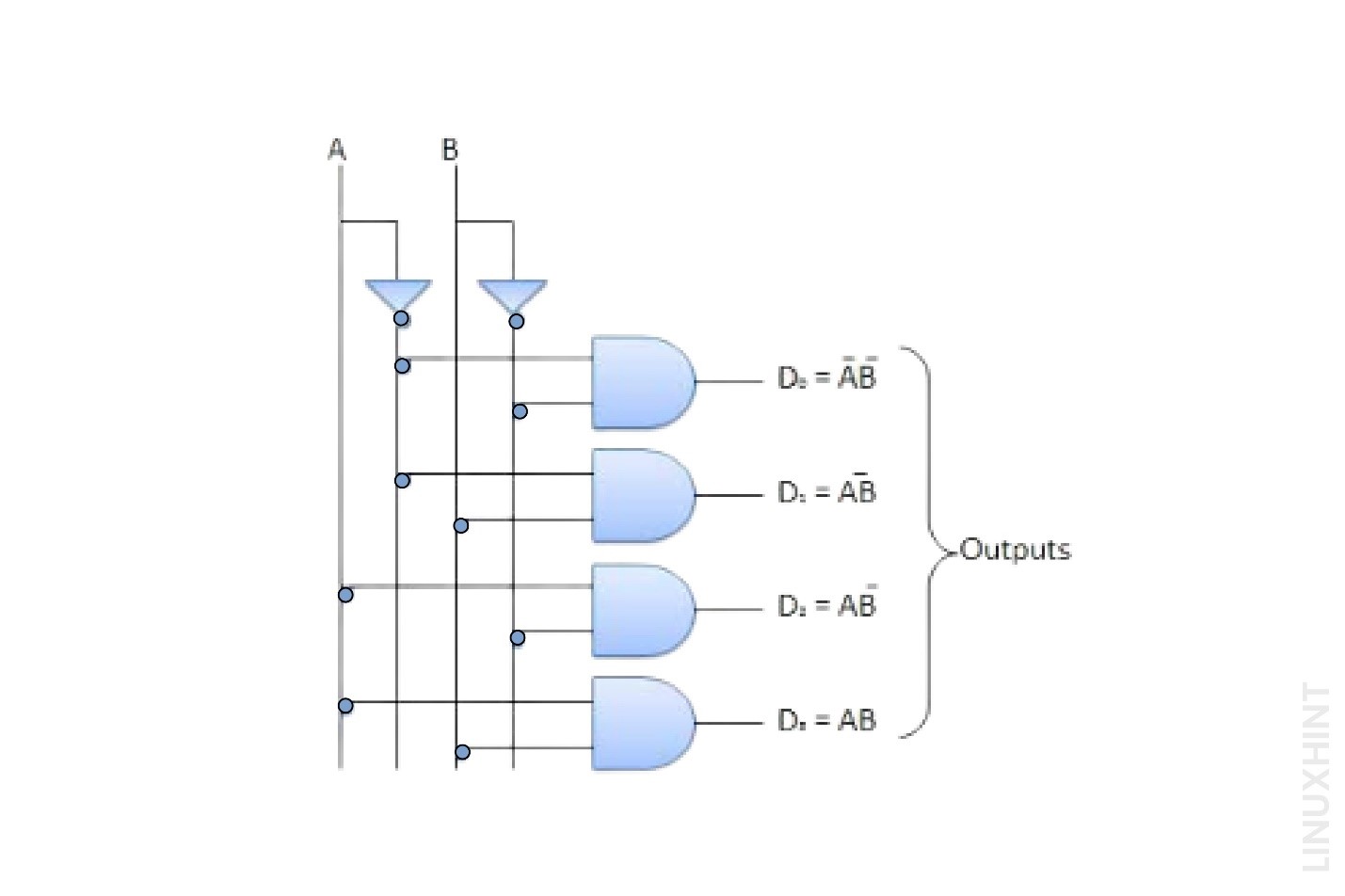
2 to 4 lines Decoder
The below decoder depicts the block diagram of a 2-to-4-line decoder. The two inputs are A and B, while the four outputs are D0 through D3. The Truth table demonstrates that each output is 1 only when a specific set of inputs is used.
Truth Table

Circuit Diagram
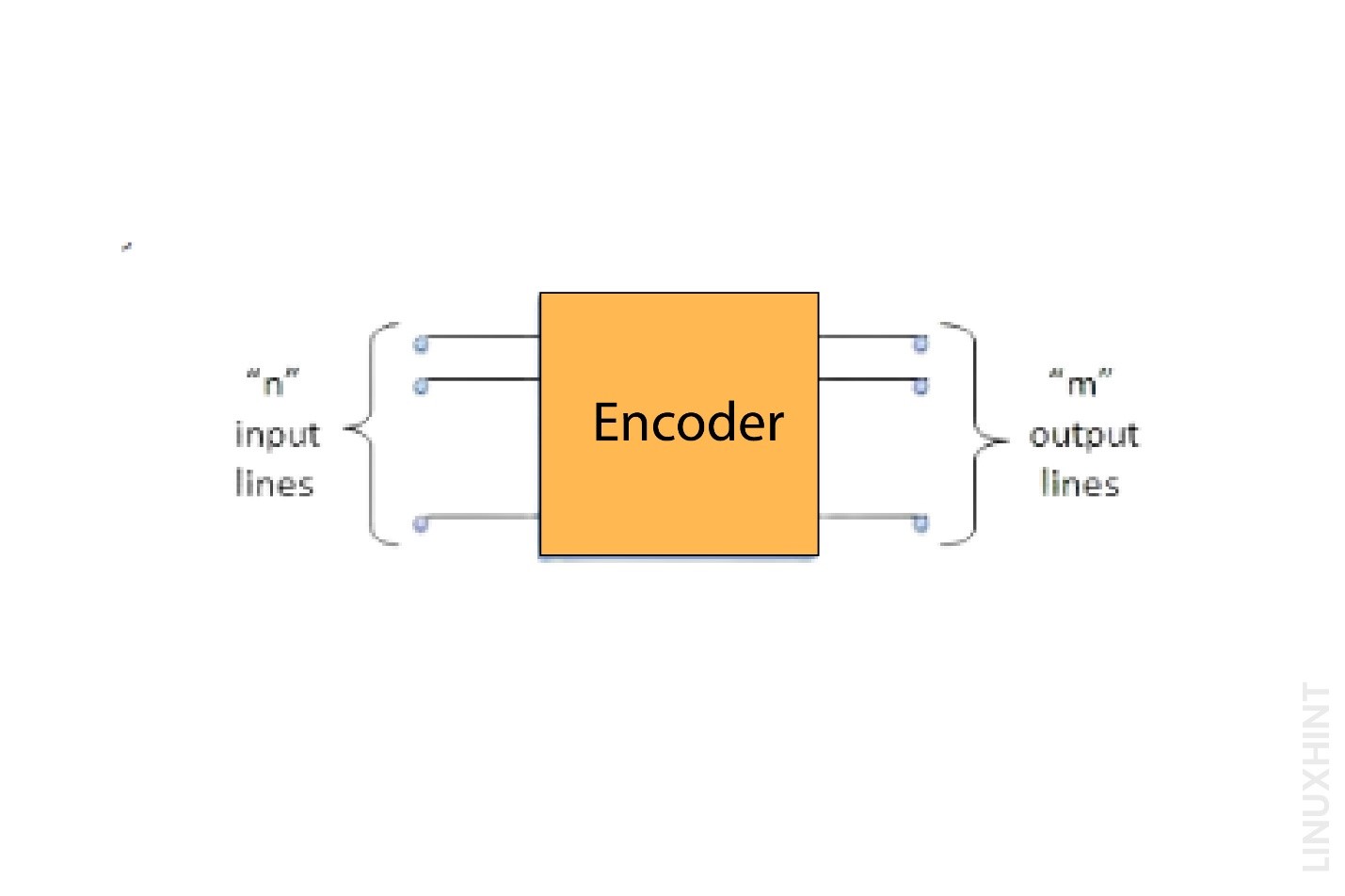
Encoder
A combinational circuit known as an encoder is created to carry out the opposite function of a decoder. There are n input lines and m output lines in an encoder. In order to represent the digital input number, an encoder generates a m bit binary code. The encoder takes an input of n digital words and turns it into a new digital word with m bits.
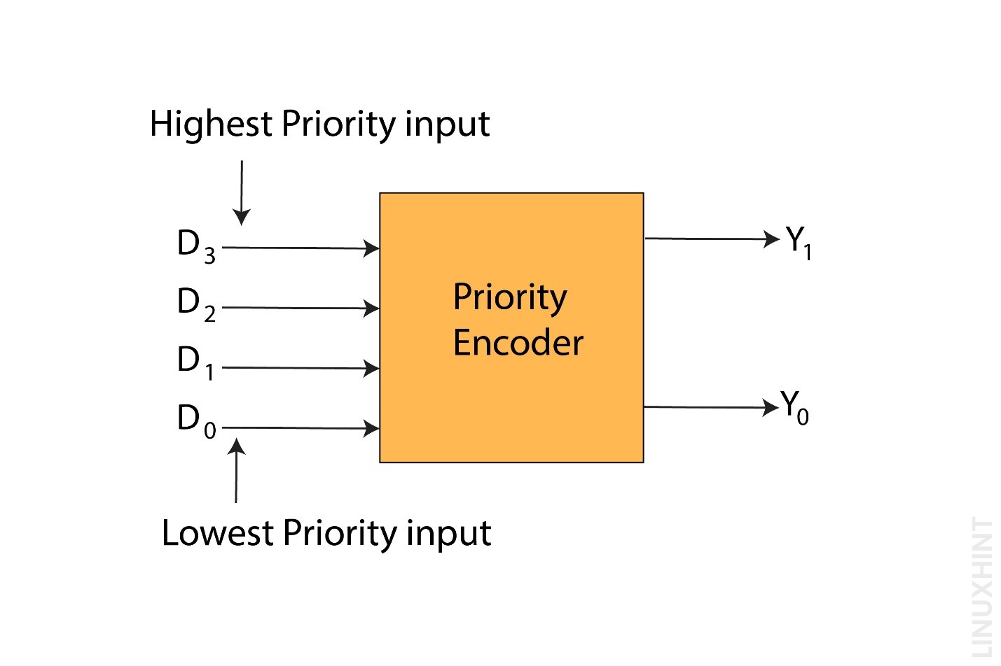
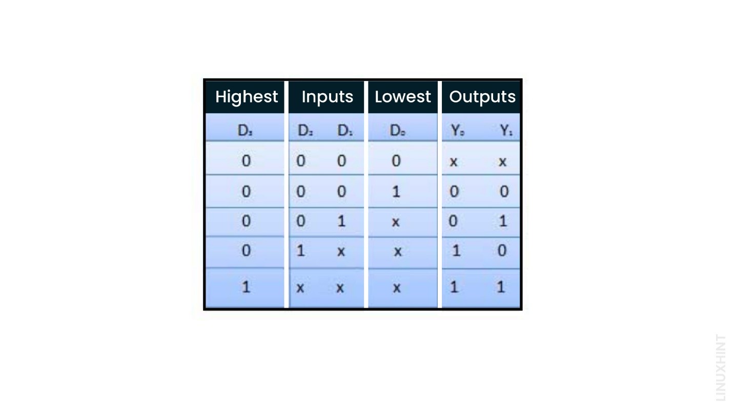
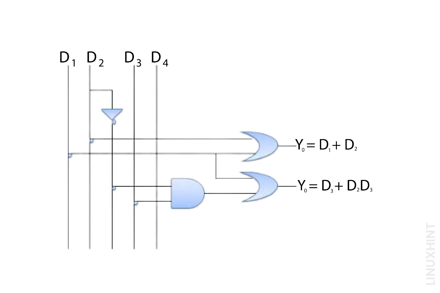
Priority Encoder
This particular encoder is unique. The input lines are given first priority. The input line with the greatest priority will be taken into account if two or more input lines have a value of 1 at the same time. There are two outputs, Y0 and Y1, and four inputs, D0, D1, D2, and D3. D3 has the most priority out of the four inputs, while D0 has the lowest priority. This indicates that regardless of the other inputs, Y1 Y1 = 11 if D3 = 1. Similarly, regardless of the other inputs, Y1 Y0 = 10 if D3 = 0 and D2 = 1.
Truth Table
Circuit Diagram
Conclusion
Combinational logic circuits can perform arithmetic functions of adders, subtractors and comparators. They also have data transmission functions such as multiplexers, de-multiplexers, encoders, and decoders. Moreover, these circuits find application as code conversion circuits.
Source: linuxhint.com